CRC-32 VLSI Design using Cadence's Virtuoso
This semester at UCF I enrolled in a 5000 level (graduate level) Very Large Scale Integration (VLSI) class entitled EEE5390 “Full-Custom VLSI Design”. It caught my eye back in the Spring of 2014 when I noticed another student’s screen as they designed a chip. The mash-up of colored rectangles and wiring intrigued me. Later I learned that the best designs would actually be fabricated through MOSIS, a university chip fabrication service. This was a big pull in my decision to take the class – how often do you get to say your design is baked in to a working piece of silicon?
With that, I decided to give it a shot this spring.
I have to say, I wasn’t disappointed. I learned more about VLSI design principals and CMOS logic than I thought I ever would as a Computer Engineering major. Overall it was a tough class as the learning curve for drawing workable circuits and proving they work wasn’t that simple. The design tools used to make transistors become a reality are from a prominent design company, Cadence.
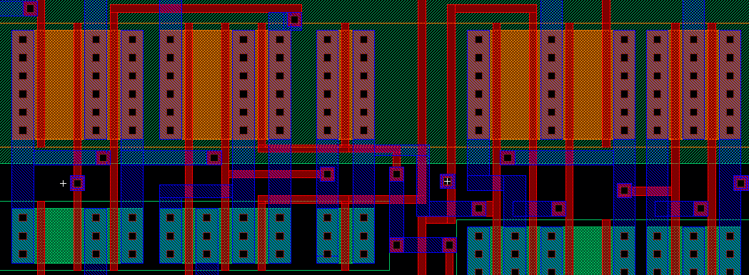
The course overview consisted of a review and derivation of the fundamental equations for PMOS and NMOS transistors, why PMOS is used for pull-up logic and NMOS for pull down, CMOS design, and finally layout. What you see in the above image is the layout stage of the design. Technically you don’t have to be familiar with the fundamental equations of transistors in order to create a working design, but for a serious VLSI designer, they are likely as important as \(V = IR \).
Before I could jump into the more advanced, global, layouts I was given a set of introductory projects. These projects had me working on specific gates such as inverters, NAND2, NOR2, XOR2, MUX2:1, and finally a negative edge triggered D-Flip-Flop. Essentially I was creating my own cell library to use in more complex designs. While doing the introductory projects, I learned the little tricks for designing and simulating the standard cells, including the hotkeys for layout.
Here is what all the background, planning and testing amounted to:
If you haven’t done any VLSI design, this appears complex and intriguing, but there isn’t any appreciation for what is actually happening. Essentially, my job is to draw metal (M1, M2, or M3) to form conductors, connect different layers using vias, and dope certain regions of the silicon substrate to create different potentials. These tasks together create transistors and the wires that connect them all together. It’s quite a beautiful process when you understand it!
First, lets start with the obvious – what do the colors represent? Here is a diagram I have created that shows the 4 main colors in the layout:
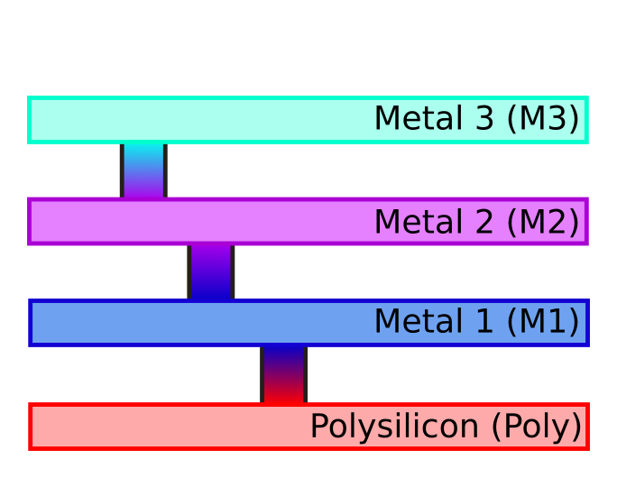
Cyan is M3, purple M2, blue M1, and red poly. M1, M2, and M3 are low resistance conductors (i.e. some metal like material) and poly is a weak conductor used for transferring logic levels to the gates of the transistors. In between each layer is a sandwich of Silicon, an insulator. When two layers need to be connected together, vias are used to electrically bond them. Without going in to further detail, using these four layers, I create wires hidden vias just like on a Printed Circuit Board (PCB).
There are some less visible layers related to the selection of dopants for the lowest layer, the substrate. These layers are used to form NMOS (light green) and PMOS (orange) transistors. I had to design my own transistors and size them right using these methods. What actually happens on a layer level is complicated and best left to the experts.1
Now, what exactly does the chip do? Well, that was up to me.
Choosing a Design
I had to decide on a design that was significant enough for a final project, yet not complicated enough that I wouldn’t be able to complete it. This ended up being a hard balance to strike, especially since I was working alone. There was the choice to work in groups, but with a class of 8, mostly non-interactive people (focused on the class, not the people in it), being in a group would just complicate matters. Plus, everyone had already learned to work well on their own.
After deliberating, I decided to go with designing the datapath of a CRC-32 checksum. I had some more complex ideas floating around in my head, such as MD5, but once I realized I would be laying out 128-bit buses by hand, I quickly moved on.
The CRC-32 algorithm is actually quite simple when using a pregenerated table. A simple C representation is shown below. 2
// 256 x 32 bit table
static uint32_t crc32_tab[] = {
	0x00000000, 0x77073096, 0xee0e612c, 0x990951ba, 0x076dc419, 0x706af48f,
        ...
	0xb40bbe37, 0xc30c8ea1, 0x5a05df1b, 0x2d02ef8d
};

uint32_t
crc32(uint32_t crc, const void *buf, size_t size)
{
   const uint8_t *p;

   p = buf;
   crc = crc ^ ~0U;

   while (size--)
      crc = crc32_tab[(crc ^ *p++) & 0xFF] ^ (crc >> 8);

   return crc ^ ~0U;
}
What was actually implemented on the chip was only a subset of the algorithm. There was no way I was going to be able to fit the CRC-32 table on-chip, therefore I had to construct a mechanism to clock in the value from off-chip. Also, to keep my design simple, I didn’t have any control logic driving the chip internally. All control signals were exported off-chip for another controller to manage. This greatly simplified the design as all I had to worry about was the flow of data from one spot to another and what structures were needed.
The CRC-32 algorithm ended up being a great choice, but it was still scaled higher than what our design process and final physical chips could handle. For one, due to the size of each CRC-32 table entry, I wasn’t able to directly read in all of the data. Instead, I used a shift register to clock in a bit per cycle. This was quite slow compared to a normal CPU/MCU, but my primary goal was a functioning design. The only reason this had to be done was primarily due to the final physical limitations of the dies and their package pin count. This is discussed further in Taping Out the Chip.
Planning the Design
Before I started laying out the chip, I made an initial design and testbench in Verilog. Jumping straight in to layout is a bad idea because forgetting one important element or caveat could change your entire design. I wanted to avoid that thru extensive planning. Verilog is best suited for planning a design like this because it directly models hardware. Now, VHDL could have also been used, but considering as I haven’t written any VHDL, that would have been a bit difficult.
In planning what my design would need, I used the above C code to translate the functionality to Verilog. From my experience in translating programs to Verilog, I’ve learned to look at the operations that the code performs at a high level and ask myself
- What operation is taking place?
- What is the width of the data required for that operation?
- Does the result of this operation require storage?
For example, in the snippet below
we can see that the CRC value coming in and going out is XOR’d with ~0U,
which is 0xFFFFFFFF. Now for a CPU, an actual xor instruction would have to
be emitted in order to perform this operation.
uint32_t
crc32(uint32_t crc, ...)
{
   crc = crc ^ ~0U; // line 14
   ...
   return crc ^ ~0U; // line 19
};
In hardware, I don’t see that as an XOR operation – I see it as an inversion. Any bit XOR’d with 1 will always be the bit inverted. This is shown in the XOR truth table below.
| 0 | 0 | 0 |
| 1 | 0 | 1 |
| 0 | 1 | 1 |
| 1 | 1 | 0 |
What this means for the design, is that instead of wasting space using an XOR gate for those two operations, an inverter will suffice.
Next, I broke down the main loop of the CRC algorithm. Now came an important decision point – do I have the loop state exist inside of the chip or outside? Written differently, do I make my chip a purpose built “CPU” that takes in a length, followed by a “length” number of bytes and spits out the CRC result? Or do I make a “dumb” chip that has all of the structures necessary to perform all of the CRC calculations, but with the control lying outside of the chip? I chose the latter due to the simplicity of the design; only a datapath is required.
Following that decision, I needed to break down the CRC algorithm in to discrete, on-chip structures – i.e. logic gates and registers. One iteration of the CRC algorithm amounts to the below
uint32_t crc = currentCrc; // 32-bit running CRC
uint8_t byte = nextByte;   // 8-bit byte

crc = crc32_tab[(crc ^ byte) & 0xFF] ^ (crc >> 8);
All of the control flow is removed and just one iteration remains. Assuming we
don’t care about the initial states of crc and byte, we can focus directly
on the logical operations needed. This snippet still isn’t fine grained enough to
start translating directly in to hardware. We need to break down that line into
more discrete actions.
uint32_t crc = currentCrc; // 32-bit running CRC
uint8_t byte = nextByte;   // 8-bit byte

uint8_t tableIndex = crc ^ byte; // uint8_t limits value to 0-255
uint32_t tableItem = crc32_tab[tableIndex];  // 32-bit array lookup
uint32_t xorResult = tableItem ^ (crc >> 8); // 32-bit XOR

crc = xorResult; // store new CRC
From the broken down version, I can now see that I need a way to store a
32-bit crc value, an 8-bit byte value, and a 32-bit tableItem value. I
could technically have another 32-bit register for storing the xorResult, but
in hardware I can make the XOR result feed directly back in to the crc
register.
In terms of operations, I have an 8-bit XOR2, a 32-bit XOR2, a shift right by 8, and a table lookup given an 8-bit index. This means I need at least 40 XOR2 gates and a way to lookup a table value from off chip. As for the shift, in hardware it’s “free” because a “shift” amounts to merely rearranging wires.
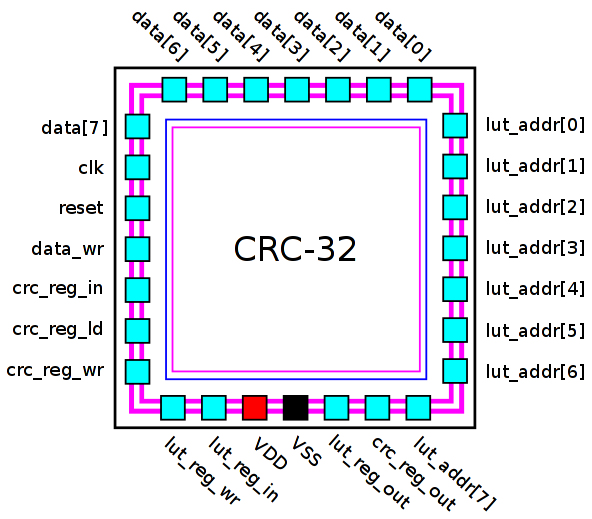
Externally, the CRC-32 design would be seen like the diagram below. This top-level module mirrors the pins that would appear on a physical chip, except for the power pins. If you were to buy a chip like this, you would see this diagram with instructions on what each of the pins mean along with what they expect.

| Signal | Bitwidth | Description |
|---|---|---|
| clk | 1-bit | Clock signal to trigger the flip-flops |
| reset | 1-bit | Reset signal to reset all on chip flip-flops |
| data | 8-bits | Bus to read in the next byte of input to be CRC’d |
| data_wr | 1-bit | Serves as a write enable for the data flip-flop |
| lut_addr | 8-bits | Output for the CRC32 table (LUT) address |
| crc_reg_in | 1-bit | Leftmost data in bit for the 32-bit crc_reg flip-flop shift register |
| crc_reg_ld | 1-bit | Toggles the crc_reg between loading a 32-bit word (1) and shifting (0) |
| crc_reg_wr | 1-bit | Write enable for the crc_reg |
| crc_reg_out | 1-bit | Rightmost output of the crc_reg. Used to shift out the CRC result |
| lut_reg_in | 1-bit | Leftmost input to the lut_reg flip-flop |
| lut_reg_wr | 1-bit | lut_reg write enable |
With this top-level view, the internals ended up like the Verilog code below.
module crc32
(
  input clk, reset,
  input [7:0] data_in,
  input data_wr,
  input crc_reg_in, crc_reg_ld, crc_reg_wr,
  input lut_reg_in, lut_reg_wr,
  output data_out,
  output crc_reg_out,
  output [7:0] lut_addr
);
  wire clk, reset; // standard signals
  wire [7:0] data_in; // data input for the CRC calc
  wire data_wr;    // data register write
  wire crc_reg_in; // crc_reg shift in
  wire crc_reg_wr; // crc_reg write signal
  wire crc_reg_ld; // crc_reg direct load
  wire lut_reg_in; // crc_reg direct load
  wire lut_reg_wr; // crc_reg write signal

  // internal wires
  wire [7:0] data_out_bus;
  wire [31:0] crc_reg_in_bus;
  wire [31:0] crc_reg_out_bus;
  wire [31:0] lut_reg_out_bus;

  sr #(8) data_reg(
    .clk(clk),
    .reset(reset),
    .ce(data_wr),
    .load(1),
    .din(0),
    .din_load(data_in),
    .dout(data_out_bus)
  );

  sr #(32) crc_reg(
    .clk(clk),
    .reset(reset),
    .ce(crc_reg_wr),
    .load(crc_reg_ld),
    .din(~crc_reg_in), // make sure the input is inverted
    .din_load(crc_reg_in_bus),
    .dout(crc_reg_out_bus)
  );

  sr #(32) lut_reg(
    .clk(clk),
    .reset(reset),
    .ce(lut_reg_wr),
    .load(0),
    .din(lut_reg_in),
    .din_load(0),
    .dout(lut_reg_out_bus)
  );

  assign lut_addr = data_out_bus ^ crc_reg_out_bus[7:0];
  assign crc_reg_in_bus =  {8'b0, crc_reg_out_bus[31:8]} ^ lut_reg_out_bus;

  assign data_out = data_out_bus[7];
  assign crc_reg_out = ~crc_reg_out_bus[31]; // invert the output
endmodule
Essentially the whole CRC-32 design consists of a bunch of Flip-Flops wired as shift registers and some XOR gates. In Verilog this is embarassingly simple, but the Full-Custom layout is far from it. 32 FFs means 32 wires going in and 32 coming out – that’s a lot of wires to route by hand and hook up. This is definitely the reason that tools are used to avoid monotonous hand routing, but in the spirit of building your own bird-feeder,3 I got to be the router.
The underlying registers were created with the sr module below. I built in
the flexibility for a specific value to be loaded instead of having to
shift one in bit by bit.
module sr #(parameter W = 2)
(
  input clk, reset, ce, load, din,
  input [W-1:0] din_load,
  output [W-1:0] dout
);
  wire clk, reset, ce, load, din;
  wire [W-1:0] din_load;

  wire [W-1:0] data_sel;
  wire [W-1:0] dout;

  assign data_sel[0] = load ? din_load[0] : din;

  // first flip-flop
  adff dff_begin(
    .clk(clk),
    .reset(reset),
    .ce(ce),
    .din(data_sel[0]),
    .dout(dout[0])
  );

  // generate all of the internal flip-flops
  genvar index;
  generate
  for (index=1; index < (W); index=index+1)
    begin: gen_code_label
      assign data_sel[index] = load ? din_load[index] : dout[index-1];

      adff dff(
        .clk(clk),
        .reset(reset),
        .ce(ce),
        .din(data_sel[index]),
        .dout(dout[index])
      );
    end
  endgenerate
endmodule
In order to have full control over every structure in the design, I ended up creating my own D-Flip-Flop which modeled the one created in Cadence. The simple Verilog implementation is below and it can be seen that it’s a normal FF but negative edge triggered with an asynchronous reset and resets to the value of ‘1’.
/* D-Flip Flop that models what has been designed in cadence
 * Asynchronous reset, enable signal, reset value of '1'
 */
module adff
(
  input clk, reset, ce, din,
  output dout
);
  wire clk, reset, ce, din;
  reg dout;

  always @(negedge clk or negedge reset)
    if (~reset) dout <= 1'b1; // reset at any time
    else if (ce) dout <= din; // new value if enabled
    else dout <= dout;        // hold
endmodule
Testing the Verilog
For each module (adff, sr, crc32), a testbench was written to test its functionality. This is standard practice in HDL as you really want to be sure things are working the way you expect them to before complicating your design. Not periodically testing modules is akin to not compling and testing regular code. Finding bugs early in Verilog saves a ton of headaches, especially when the entire system assumes the correct operation of the underlying modules. Try debugging a CRC-32 algorithm when your Shift-Register has an off-by-one – good luck with that. All of the testbenches are included with the full Verilog source as an attachment at the end of the post. In a final taped out design, the testbench will have to implemented in the real world using an Arduino or similar device.
The primary crc32 testbench manipulates the control signals and feeds data in
as needed. The primary states for performing a full CRC-32 are shown in the
state diagram below.
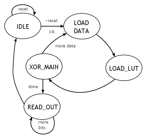
When exiting the IDLE state, the machine begins in LOAD_DATA. This is where one byte is clocked in to the data_reg. This kicks off an on-chip combinatorial XOR in parallel. Once all 8-bits of data is clocked in, the result of this XOR is read out from the lut_addr IO. Using this address, the corresponding lookup-table value is read. This brings the state diagram to LOAD_LUT, in which all 32-bits of the LUT value will be clocked in to the lut_reg. While this value is being clocked in, the 32-bit XOR gate is firing and calculating the next CRC value. Once all bits are clocked in, the chip enters the XOR_MAIN state. When the combinatorial XOR output settles, crc_reg_ld is brought high to signify that a direct 32-bit load will take place next clock cycle. The chip is clocked and if there is more data to read, the state machine continues with LOAD_DATA. Else it will end with READ_OUT until a chip reset. READ_OUT allows for the crc_reg to be clocked out back to the controller for further usage.
Once the glue and flow of the state machine was settled, data was read from and written to the underlying Verilog module to simulate a complete CRC-32. Once the outputs matched that of the golden module (the C program from the beginning), I stopped simulation and moved on to laying out the design.
Designing the Chip Layout
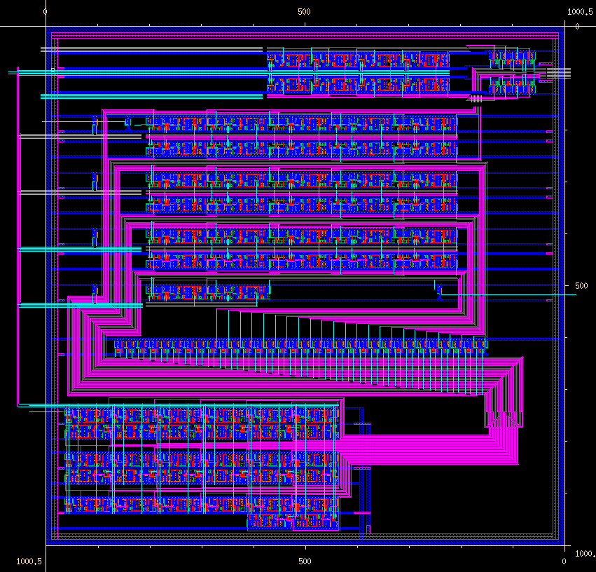
The above should attest to the complexity involved with even the most simple chips. Being able to talk about a few flips flops and XOR gates for the amount above goes to show you really do need advanced methods of development or a lot of people to get complex designs done quickly. With all of the foundation laid out, I was able to jump straight in to the labor intensive task of placing and routing the layout.
First, I created a basic power frame for my chip. This merely consists of a Vdd (+5V) and a Vss (ground) square. Later this will need to be attached to an actual pad frame, which physically connects internal nets to bonding pads. Metal 1 (dark blue) was used for Vdd and Metal 2 (purple) for Vss. Note: there is a convention in which M1 and M2 should always be perpendicular. I loosely followed this convention as the design will illustrate.
To help show the major structures on the top-level diagram above, I hastily drew some ugly solid color boxes to denote each register and XOR block.
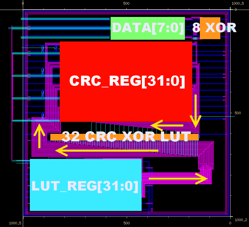
From the above diagram, I can count the major structures implemented on chip
- 2x 32-bit registers
- 1x 8-bit register
- 32x 2:1 MUX’s
- 1x 8-bit XOR2 array
- 1x 32-bit XOR2 array
- 6x inverters
- Global routing
See if you can spot the inverters.
Once again, the design at a high level wasn’t so bad, but the 32-bit routing
nearly killed me. It’s a structure in itself. As you can see, there are two
major buses that converge in the center to perform a big 32-bit XOR. This
result then gets fed back in to the crc_reg in the middle. That alone was quite
difficult as managing the space I had became quite difficult with 32 wires to
route in parallel. To avoid the global routing nightmare and obvious pin
limitation, crc_reg and lut_reg are shift registers. crc_reg can convert
to a directly loaded register due to the MUX2:1’s that are in front of each
flip flop.
Testing the Chip
Testing a final laid out design is more difficult than a simple Verilog version. This is primarily due to the fact that Cadence doesn’t provide any digital abstraction that I could easily find. I suspect that this is due to Cadence being a popular analog design tool and the fact that this is full custom after all. Essentially, all simulation is done using transient analysis and raw waveforms. This would not scale for more complex designs, but for the purposes of this design and the class, more advanced methods, such as Verilog testbenches in Cadence, were not investigated.
Once a my design was finalized and all of the important nets named, I extracted the design in order to instantiate a SPICE model that also included parasitic capacitances. From here I used the standard tool ADE L to create input stimulus and view the resulting outputs. This was mildly painstaking as I had to manually enter, bit by bit, what I wanted each signal line to be driven to. This is all while manually syncing the clock signal and reset line.
An example of the output for a simulation waveform is displayed below.
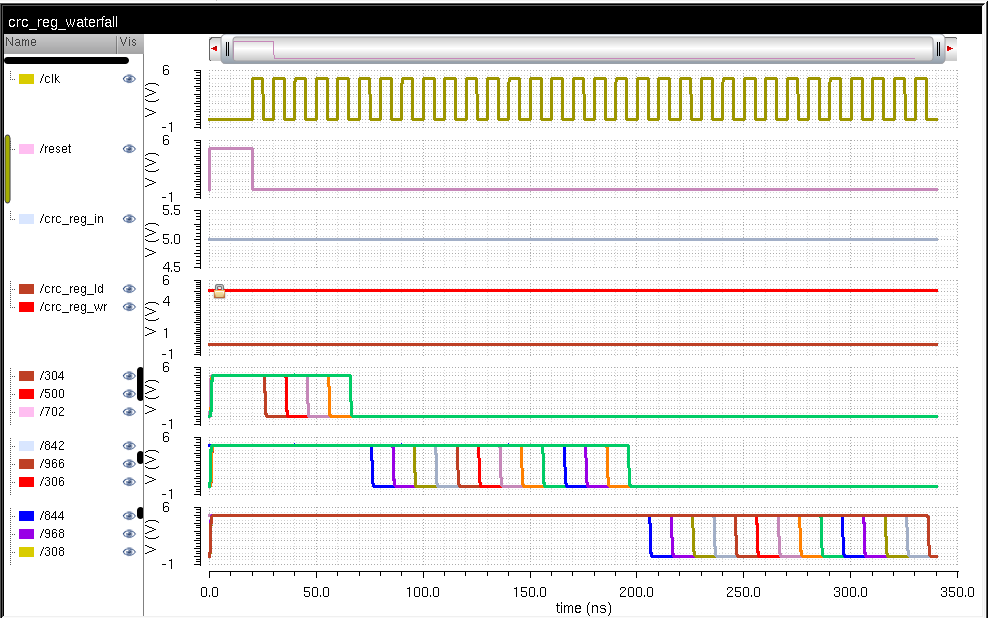
It just shows me testing the crc_reg’s shift register capability. I hold the
crc_reg_in line to one and continually clock the chip. This makes a series of
ones fill up the shift register.
Long story short, I successfully tested each register for its functionality.
From this testing, I ended up fixing a fatal error where I incorrectly hooked up the out pins
of the MUX’es to the inputs of the crc_reg flip-flops. Before then the FF inputs weren’t being
driven, so my results were very strange.
Taping out the Chip
After the long and arduous process of planning, designing, and testing the time arrived to submit my design to MOSIS for fabrication. The fabrication used was SCN3ME_SUBM, which is a \(0.3~\lambda\) process. In order to target that process, our class used NCSU’s CDK. This CDK plugs straight in to Cadence and allows for designers to target the AMI 06 process without having to worry about all of the nitty gritty details of the process.
The final design came out to be \(1484.4 \times 1484.4~\mu m\) (area of \(2.203~mm^2\)). I should be getting 5 taped out DIP-28 packaged around August. Looking forward to that!
The final pad frame and filled design (due to layer density requirements) are shown below:
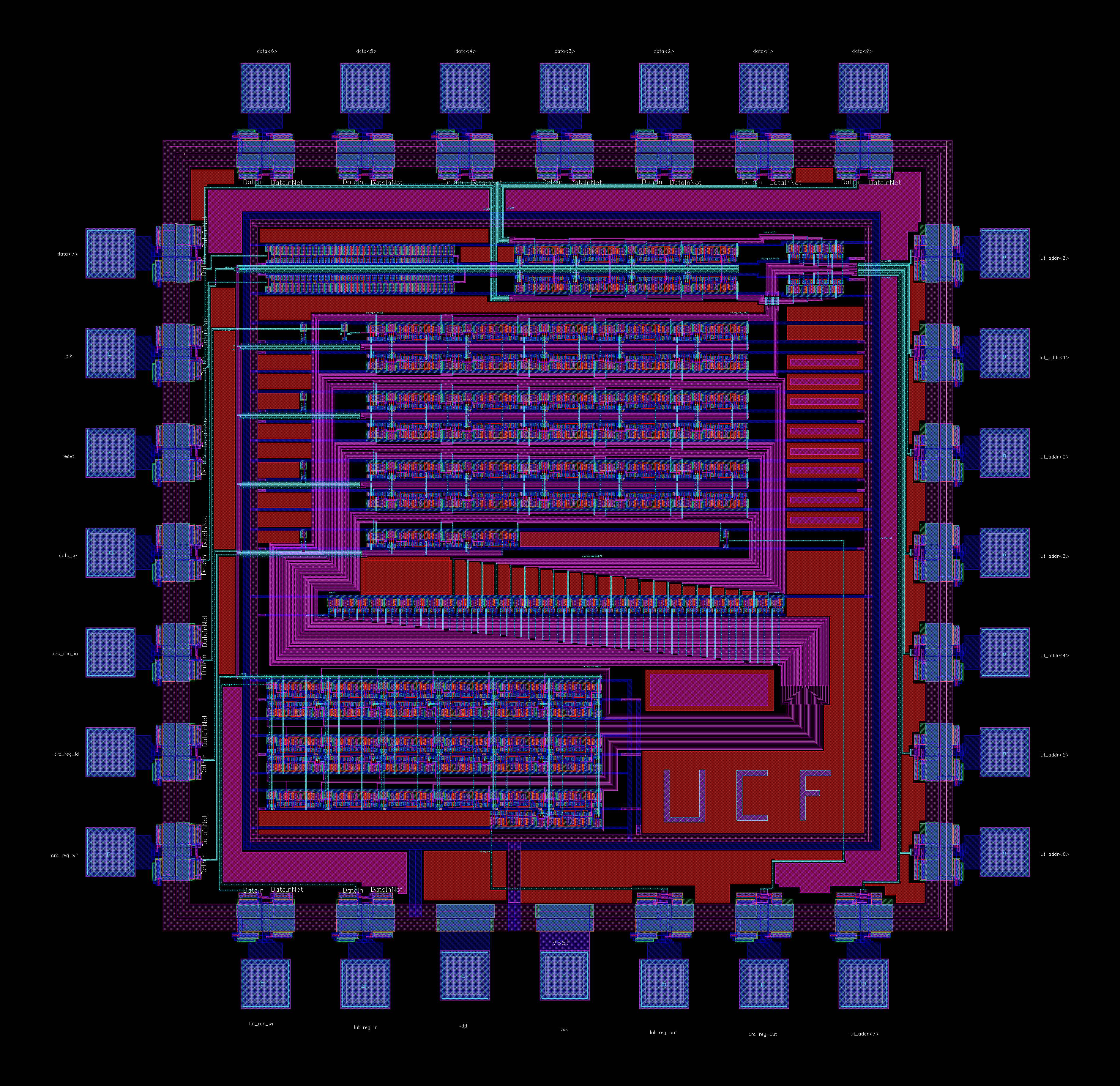
(click for hi-res version)
For any people new but interested in VLSI design, I hope you gained some insight in to how to think about creating a chip of your own from start to finish. For everyone else: Beware - here be dragons.